Originally Posted by
borescopeit

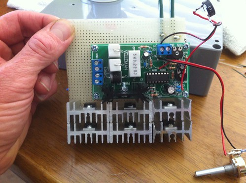
My POWER MOSFETS end up in smoke!!! Any idea?
Here is my setup:
I run a dry cell capable of consuming 350 amps, feed it with 14.2VDC from 220AMP Delco heavy duty alternator through #4 OFC wires that handle around 70 amp (this is the amps the cell runs at). Will upgrade my wires to #1 welding cables (will carry through up to 150 amps).
My KOH e-lyte is at 21%.
POWER MOSFET is ON Semiconductor NTB125N02R capable of driving 125A 24VDC @ 25C.
When I run it at 100% duty @ around 20KHz (it is that fast to handle up to 5 MHz) everything is just fine, being cooled by 12V 2" fan stays at 35C, but when I lower its duty cycle it immediately heats up to 102C and if I do not shut it off on time it ends up in a garbage bin.
Does anybody experienced the same sh1t?
Should I try lower switching frequency while lowering its duty cycle? I use microcontroller to drive the FET so I can preset any frequencies. Best freq. I found to be for my cell is around 3.6 & 23 Khz.
Also, I am playing with alternating two different freqs. every X seconds.
Any advice is appreciated!


 Reply With Quote
 ). If I fail to cool down this much heat the FET will be kaput.